
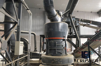
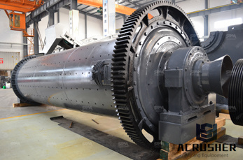
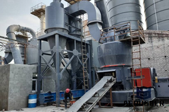
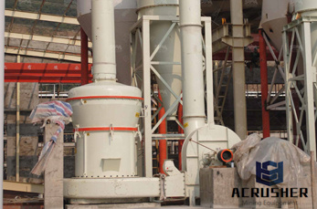
Wafer Back Grinding Process manufacturer Grasping strong production capability, advanced research strength and excellent service, Shanghai Wafer Back Grinding Process supplier create the value and bring values to all of customers.
 WhatsApp)
Effect of Wafer Back Grinding on the Mechanical Behavior of Multilayered Lowk for 3DStack Packaging ... generated during wafer back grinding process affect the.
Effect of Wafer Back Grinding on the Mechanical Behavior of Multilayered Lowk for 3DStack Packaging ... generated during wafer back grinding process affect the
Warping of silicon wafers subjected to backgrinding process ... grindingbased backthinning process is featured with a ... act on the wafer subjected to backgrinding,
Leadingedge Tape B!_ (B Equipment solution created with semiconductorrelated products ''Adwill.'' Fully and semiautomatic wafer mounters for the dicing process.
Wafer Backgrind is the process of grinding the backside of the wafer to the correct wafer thickness prior to assembly. It is also referred to as ''wafer ...
Dicing Grinding, Greases, Gels Wax Coatings. Wafer Dicing Tapes; ... Wafer Back Grinding Tapes. ... Consistent bond strength during grinding process;
Numerical Simulations of a Back Grinding Process for Silicon. Publication » Numerical Simulations of a Back Grinding Process for Silicon Wafers.
The TAIKO process is the name of a wafer back grinding process that uses a new grinding method developed by DISCO. This method is .
A wafer sawing/grinding process capable of removing cracks and chipping resulted from a wafer sawing operation. A silicon wafer having an active surface and a back ...
Backgrinding. Backgrinding is the process of ... Final outgoing inspection is then carried out before the lot is prepared for shipment back ... Finally, the wafer is ...
Figure 1. a) A backgrinding process leaves a characteristic scratch pattern on the back of the wafer. b) The back of the die from certain locations on the wafer have ...
Plasma systems for wafer stress relief ... process containing no free ions or electrons that could potentially charge the surface of the wafer. The backgrinding ...
Silicon Wafer Back Grinding Wheel Features Thoroughlymonitored manufacturing process for nearzero scratch Manufactured in clean room class: 100 ~1000
Dec 02, 2014· Grinding a 25Inch F3 Telpe Mirror: Thinning and Flattening the Back Duration: 10:59. GordonWaite 103,343 views. 10:59. Wafer Dicing Process ...
parallelism between the front and the back surface. Secondly, the grinding ... achieve this we need to understand thoroughly the process of semiconductor wafer grinding
Wafer Pick And Place Service Grinding and Dicing This process allows you to extract particular die from a wafer and place them back on Wafer Grinding Polishing ...
Wafer backgrinding is a semiconductor device fabrication step during which wafer thickness is reduced to allow stacking and highdensity packaging of integrated ...
Syagrus Systems thin wafer backgrinding and silicon wafer thinning services meets ... more about our Wafer Dicing Process. ... your next back grinding wafer ...
Effects of back grinding process on ... read more; Wafer dicing,Wikipedia, ... The process of wafer backgrinding induces stress that can propagate into the bulk of ...
Custom Silicon Wafer Back Grinding Services SVM. Back grinding is a process that removes silicon from the back surface of a wafer Silicon Valley Microelectronics ...
BackSide Wafer Grinding Quality Affecting BackEnd Assembly, back grinding process,ABSTRACT Die size and thickness of IC .
GDSI, Grinding and Dicing Services complete resource for Silicon Wafers Processing includes Probing, Bumping, Grinding, Polishing in San Jose, California.
Semiconductor BackGrinding The silicon wafer on which the active elements are created is a thin circular disc, typically 150mm or 200mm in diameter.
The present invention relates to a process for the backsurface grinding of wafers using films which have a support layer, which is known per se, and an adhesion ...
WhatsApp)